


 Home
Home a
a
a Department of Medical and Industrial Materials Science, College of Applied
Science, University of Technology- Iraq
b Department of Laser Science and Technology, College of Applied Science,
University of Technology- Iraq
c Applied Science Research Unit, College of Applied Science, University of
Technology- Iraq
Journal of Ovonic Research 2025, 21(6),725-739; https://doi.org/10.15251/JOR.2025.216.725


An inclined-angle chemical spray pyrolysis method deposited 3.0% Al-doped CdO thin films on two types of substrates (silicon and glass). The films showed high conductivity, stable cubic structure with dominant (200) orientation, and homogeneous spherical grains of 100–200 nm. Their visible absorption coefficient was ~104 cm–1 and bandgap 2.29 eV.
Two heterojunctions n-CdO/n-Si and n-CdO/p-Si were fabricated. The n-CdO/n-Si junction exhibited rectifying behavior with a reverse-bias gain of 6.7, visible-light detection, and low resistance. n-CdO/p-Si junction achieved a photoresponse of 18×10–4 A/W at 520 nm compared to 5×10⁻⁴ A/W. These characteristics make the films promising for optoelectronic applications.
Nanostructured materials have received growing interest lately through their vital role played in enhancement of technological applications, and production of advanced materials that have outstanding physical and chemical properties [ 1-3]. Eventually, metal oxides have drawn much attention for their contribution in cutting-edge applications related to electronics, photovoltaic, and sensing devices [4]. Examples of these metal oxides such as cadmium oxide, zinc oxide, titanium oxide, and indium tin oxide. They showed high competency in specific applications of dye- sensitized solar cells (DSSC) [5], and photoelectrochemical cells (PECs) [6]. Cadmium oxide (CdO) film has unique characteristics. It is an n-type semiconductor with a favourable bandgap energy within (2.2–2.7) eV in the visible region, and a high electrical conductivity of (102 - 104) S/cm. It is also a semi-transparent material in the visible and near infrared (NIR) regions [7- 11]. It is a promising semiconductor based on its dual combination of transparency and low electrical resistance [7, 8, 12].
Moreover, CdO deposited on silicon exhibited remarkable optical and electrical properties
[ 13]. As a result, CdO has become an indispensable candidate in across a broad spectrum of optoelectronic applications like humidity sensors, solar cells, photodiodes, phototransistors, transparent electrodes, and IR detectors [ 14- 16]. Adding dopants (for example Sn, In, F, Cu, Ga, and Al) to CdO thin films increases the electrons concentration and improves their electrical conductivity [9, 12, 17- 20]. Although few studies are reported for Al-doped CdO films, Aluminium was successfully employed to dope other transparent conductive films in order to improve electrical conductivity, and increase the concentration of conduction electrons [ 12, 19, 20].

* Corresponding author: mustafa.a.hassan@uotechnology.edu.iq https://doi.org/10.15251/JOR.2025.216.725
Numerous techniques were implemented for preparing pure or doped CdO thin films. Among these techniques: sol-gel [21], SILAR [22], thermal evaporation [23], electron beam technique [24], pulsed laser deposition (PLD) [25], sputtering [26], chemical vapour deposition (CVD) [27], and chemical spray pyrolysis (CSP) [ 11, 12]. Remarkably, each technique is unique in its yield, benefits, and drawbacks. Notably, CPS offers several advantages, including simplicity, cost-effectiveness, vacuum-free operation, and suitability for industrial fabrication, easiness in adding doping materials, repeatable, films quick growth, and possibility of achievement a homogenous film surface [ 11, 28]. A number of research work was disseminated regarding the formation, characterization, and efficiency of CdO nanostructures for diverse applications. For instance, CdO nano-sheets were generated hydrothermally by N. A. Shad et al. [29], who also proposed that CdO nano-sheets were great photo-catalyst materials for the photo-degradation of toxic organic when exposed to UV light. R.N. Bulakhe and his colleague [30] prepared cubic- structured CdO thin films using chemical bath deposition (CBD). They concluded that the synthesized thin film was a highly sensitive substance for liquefied petroleum. Consequently, the film can be employed as a gas sensor. Using the sol-gel method, F. Yakuphanoglu [31] prepared a nanocluster CdO thin film. It was deduced that this film was a good nominee for an effective solar cell device. Another research group was used CSP technique to prepare Al-doped CdO thin films. They found that using Al was efficiently improved the CdO linear optical characteristics and emphasized a significant impact on their structural and morphological characteristics. The most important outcome associated with this study was the possibility of utilizing the prepared films in promising applications represented by optoelectronic gadgets [32].
By using the same deposition technique, Azzaoui et al. were recently examined what happens to CdO thin films when both aluminium and tin are added during deposition onto glass at 350°C. They reported that co-doping with these elements enhanced the physical properties of CdO thin films [33].
Although several reports [ 12, 19,34] studied electrical and optical behavior of Al-doped CdO films, studies specifically focusing on their properties when deposited on Si substrates via the CSP method remain limited. The final product's characteristics can be significantly influenced by adjustments to the substrate's tilt angle during film growth, regardless of the deposition method.
In previously published studies, the co-authors synthesized films using the CPS method at a tilt angle of 45 degree [ 12, 35, 36]. Compared to films deposited via the conventional vertical chemical spray method [37], those prepared using a tilted configuration exhibited improved uniformity, as the reduced droplet impact energy on the substrate contributed to smoother and more homogeneous films. In this context, Al-doped CdO thin films were fabricated via CSP at a deposition angle of 45 degrees, followed by optoelectronic characterization. Two prior studies [12, 23] systematically optimized Al doping in CdO, identifying 3% and 5% as the optimal concentrations for enhancing electrical conductivity while minimizing structural defects. Consequently, this study adopts comparable high doping levels and annealing treatments to further investigate their effects on CdO-Si junctions for optoelectronic applications.
CdO thin films doped with aluminum (doping ratio 3%) with enhanced electrical conductivity of semi-degenerated 3% Al doped CdO thin films were prepared using CSP technique. This was done to explore the possible applications of these films in heterojunction photodetectors. Two types of silicon wafers (n-type and p-type) were used as substrates. The orientation of the wafers was (111), the thickness was 550μm, the sheet resistance varied between (1-4) Ω/□, and the doping concentration was approximately 2.3 × 1017 cm-3. CdO precursor was a solution of cadmium nitrate of (0.2 M) which was prepared by dissolving [Cd (NO) 3. 4H2O], and [(Al (NO3)2.9H2O] in deionized water. The optimal solution composition for 3% Al: CdO film deposition was obtained by mixing a 0.2 M cadmium nitrate solution of 97 cm-3 with 0.2 M aluminium nitrate solution of 3.0
-3
cm .
The dimensions of the slides used for optical microscopy investigation were (2.5 × 2.5) cm² . The n-type and p-type silicon wafers were also cut to be with an area of(1.0 × 1.0) cm² . Prior to thin film deposition process, the silicon substrates underwent a 10-minute immersion in 5.0% HF to eliminate the native oxide thin layer. Glass and Si substrates were washed using ethanol and distilled water, and special tissues were used to dry them. Figure 1 shows the CSP setup used to prepare samples. The substrates were placed on a hot plate for warming them up to 400°C. The prepared solution was sprayed for a spray time of 4.0 s at an angle of 45° . The time interval between each two sprays (stoppage time) was 30s. The air compressor was adjusted at 6.0 kg/cm², and the nozzle is fixed a distance 30 cm from the substrate. When the deposition process was completed, the films were annealed for two hours at 400°C to eliminate any internal stresses caused by the successive cooling and heating. Following deposition and annealing, the films were subjected to various characterization techniques to assess their structural, morphological, and optoelectronic properties. The crystal structure was analyzed using X-ray diffraction (Shimadzu 6000, CuKα1, λ = 0.15406 nm). Field emission scanning electron microscope (FESEM) was used to characterize the surface morphology. (Model: Mira3, Tescan). The optical properties are tested by a UV-Vis spectrometer (Metertech SP8001), and the dark current-voltage characteristics are measured by DC power supply and an electrometer. The tungsten-halogen lamp was used to illuminate the samples under the I-V characteristics, and a monochromator was used to measure the spectral response (responsivity) of the CdO/Si heterojunction detectors.
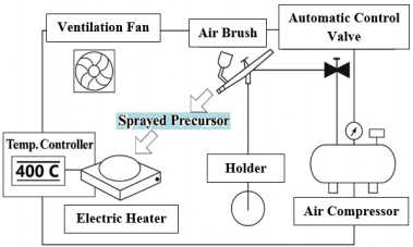
Fig. 1. Experimental setup for CSP technique.
Figure 2 demonstrates the peaks of X-ray diffraction for 3.0 % Al: CdO prepared by tilt spray pyrolysis method. The XRD pattern displays three characteristic peaks at 2θ=32.92o, 38.24o, and 55.29o for the planes (111), (200), and (220), respectively. These peaks are identified by comparing them with the JCPDS card number 75-0591 [38]. Since no indication about the presence of Al₂O₃, the obtained peaks are considered as fingerprints for a highly polycrystalline pure CdO compound without detectable aluminium oxide. The absence of aluminium oxide peaks is ascribed to the employment of a very small amount of Al as a dopant. The highest intensity peaks of Al: CdO film are located in (111) and (200) planes. Consequently, the preferred orientation of crystal growth is found at these crystallographic planes. The degree of crystallisation for the plane (111) is marginally higher than the same plane reported in the previous work [ 12], whereas the degree of crystallisation for the plane (200) is quite like that work. The enhanced crystallinity can be assigned to the leaving of the films after deposition for a couple of hours on the hot plate (annealing process) for removing the internal stresses generated by alternating spraying.
The size of crystallite (D) is calculated using Scherrer’s equation [39,40]:

θ is the Bragg’s diffraction angle, λ is the wavelength of the x-ray, β is the full width at half- maximum of diffraction peaks. Table 1 below summarizes the findings of XRD test.
I (a.u.)
Fig. 2. X-ray diffraction peaks of 3%Al: CdO thin film prepared by CSP technique.
Table 1. Results obtained from X-ray diffraction test for 3.0 % Al-doped CdO prepared by CSP technique.
|
|
|
|
|
|
|
|
|
|
|
|
|
|
|
| ||
|
|
|
| ||
|
|
|
|
|
|
|
|
|
|
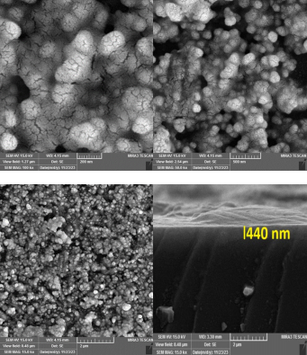
(c) 2.0 μm (d) Cross-section micrograph
Fig. 3. FESEM images for 3.0% Al-doped CdO prepared by tilt CSP technique.
Figure 3 shows FE-SEM micrographs ofa 45-degree tilt spray pyrolysis-deposited 3.0 %Al: CdO thin film on a glass substrate. Micrographs of Al: CdO thin films shows that the film is consist of spherical-like structures that have homogeneous grains, and the size is vary between (100-200) nanometres. A closer observation for the highly magnified micrographs shows that these grains are consistently overlapped or combined compared to reference [ 12]. This outcome can be linked to the annealing process. The majority of Al: CdO film grains have a monoclinic morphology. Moreover, they are dispersed throughout the surface of the film. It is observed that certain grains have cracks. In fact, these are imperfections, and they might be developed because of the alloying process. Figure 3d display a cross-sectional view of the deposited film of thickness 440 nm.
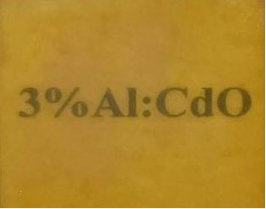
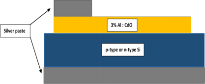
Figure (4a) depicts a photographic image of cadmium oxide film on a glass slides substrate. The film has a thickness of 440 nm and is yellow with good transparency because it displays the sample preparation condition “3.0% Al: CdO,” Figure 4b shows a device structure which is used to examine I-V characteristics and responsivity.
Figure 5 reveals the absorption coefficient (α) values calculated from transmittance data for aluminium-doped cadmium oxide thin film. The value of α increases with photon energy (ℎv) in a manner analogous to that of normal semiconductors. The figure shows high values of absorption coefficient in the order of 106 m- 1 with a rapid increase with photon energy [ℎv = 2.29 eV] , which is favourable for visible light detectors [ 1].
(b)
Fig. 4. (a) Photographic image for a glass substrate CdO thin film on it. The text 3.0%Al: CdO is written
behind the film. (b) Device structure
α (cm- 1)
Fig. 5. Absorption coefficient vs photon energy for 3% Aluminum doped CdO thin film.
Figure 6 displays the behaviour of squared absorption coefficient (αℎv)2 with photon energy(ℎv). According to Tauc’s analysis [39], the linear relationship between (αℎv)2 and ℎv suggests direct bandgap (Eg =2.29 eV) for 3.0% Al-doped CdO with predominant allowed transition
1
 type
suggesting r = 2 in Tauc’s equation [41]:
type
suggesting r = 2 in Tauc’s equation [41]:
(αℎv) = (ℎv __ Eg)r (2)
(αhυ)2
Fig. 6. (αℎv)2 vs photon energy ℎvfor 3% Aluminum doped CdO thin film.
This result is compared with earlier published data which obtained using various techniques and varied dopant ratios. Table 2 shows the reported data with reporting the required comparison.
Table 2. Comparative estimate of the energy bandgap of Al-doped cadmium oxide thin film in this method
and previously published works.
|
|
|
|
|
|
|
|
|
|
|
|
|
|
|
|
|
|
|
|
|
|
|
|
|
|
|
|
The extinction (attenuation) coefficient (ĸ) in relation to incident photon energy is plotted in Figure 7. Using the relationship (ĸ = αλ/4π) [43], the ĸ-values are computed from the absorption coefficient data. As previously shown in Figure 5, the data show that ĸ for Al-doped CdO is relatively low, with values less than 0.4 in the visible region (ℎv = 1.8-3.1 eV). This helps to explain why 3.0% Al: CdO thin films have good transparency for thickness (440 nm).
Fig. 7. Attenuation coefficient for 3.0% Al doped CdO thin film prepared by tilt CSP technique.
Ln (σ)
Fig. 8. DC conductivity for 3.0% Al doped CdO thin film prepared by tilt CSP technique.
Ln (σ)
-7.0
Ln (σ)
-11.0
(b) p-Si

1000/T (K)-1
1000/T (K)-1
κ
Figures 8 and 9 show DC measurements for 3.0% Al: CdO, n-Si, and p-Si, respectively. The natural logarithm of DC conductivity is drawn as a function of inverse temperature (1000/T) for 3.0% Al: CdO thin films. The linear proportionality between ln σ and 1000/T is concluded from a modified form of Arrhenius equation: [44]
σ = σ0 exp (__Ea /KB T) (3)
where Ea is the difference between conduction band energy and Fermi level energy, i.e., Ea = Ec __ EF for n-type semiconductor, and Ea = EF __ Ev for p-type semiconductor, KB is Boltzmann constant and T is the temperature in Kelvin unit.
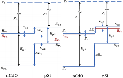
Fig. 10. Band diagram plot for n-CdO/p-Si and n-CdO/n-Si junctions, V0 is the vacuum level. x1 and x2are
electronic affinities of n-CdO and Si material respectively.Eg1 and Eg2 are the bandgap energies. EF1and
EF2 are Fermi levels. Ea1 and Ea2 are the activation energies.
The values of activation energy for n-CdO (Ec __ EF = 0.0064 eV), n-Si (Ec __ EF = 0.157 eV), p-Si (EF __ Ev = 0.349 eV) are determined from Equation (3) using the concept of activation energy. The activation energies for CdO and Si are calculated from the corresponding slopes in Figures 8 and 9 using the equation Ea = slope * 0.086. The results of DC conductivity are used in
Table 3 to evaluate the parameters, and to draw the band diagram for n-CdO/n-Si and n-CdO/p-Si heterojunctions.
Table 3. Parameters used toplot band diagram for nCdO/pSi and nCdO/nSi junctions.
|
|
|
|
|
|
|
|
|
|
|
|
|
|
|
|
|
|
|
|
|
|
|
|
|
|
|
|
|
Figure 10 confirms that the type of n-CdO-pSi, and n-CdO-nSi is staggered (Type II) where ΔEv > ΔEg . In Table 3, conduction and valence band offsets are calculated using the following equations [42]:
ΔEc = x1 __ x2 (4)
ΔEv = (x1 + Eg1) __ (x2 + Eg2) (5)
I ( μA)
I ( μA)
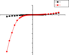
Fig. 11. I-V characteristics of 3.0% Al: CdO/Si devices. (a) n-CdO/p-Si, (b) n-CdO/n-Si
Figure 11 (a and b) demonstrates the I-V measurements for the junctions n-CdO/p-Si, and n-CdO/n-Si; respectively. The first junction, which is n-CdO/p-Si, shows an obvious rectifying behaviour under the influence of illumination condition rather than the dark condition. Notably, n- CdO/p-Si junctions exhibited a response to illumination under reverse bias, whereas n-CdO/n-Si junctions showed no significant response in either reverse or forward bias.
For the analysis of the current -voltage (I-V) measurements, it is assumed that the conduction mechanisms in these junctions are mostly controlled by thermionic emission. The junction current is given by [44, 45]:

where v is the applied voltage, q is the electron charge, n is the ideality factor for heterojunction structure, KB is Boltzmann constant, and T is the absolute temperature. Is is the saturation current, which can be evaluated using the following equation [44]:

where A* is Richardson constant for silicon, and vbi is the built-in potential. Regarding the forward bias, the association of the current with the voltage is evaluated by an exponential function, or I ~ exp (qv/nKT) [44, 45]. It is concluded from Figure 11 that the reverse current increases linearly with the applied voltage, and it does not saturate at higher voltages as indicated by Eq. (7). The symmetry ofI-V characteristic at low voltages (< 1.0 Volt) might be assigned to the localized states related to the presence of the defects, which is connected with the relatively high doping concentration of Al in n-CdO thin films (3.0%). The results of I-V characteristics are in good agreement with those of n-ZnO/p-Si [46]. The junction parameters are presented in Table 3.
As displayed in Figure 11 (b), the second junction of n-CdO/n-Si shows a rectifying behaviour for both dark and illumination conditions. Table 4 elucidates some parameters for the two junctions. IR/IF is the absolute ratio of the reverse current to forward current at applied voltage of (1.0 Volt) for both dark and illumination conditions. Rs and Rsh are respectively the series and the shunt resistance for the heterojunction. The gain can be defined as the ratio of the photocurrent to the dark current. For comparison, the gain of the first junction n-CdO/p-Si in the reverse bias is higher than that one related to the junction of n-CdO/n-Si. This finding may be linked to the width of the depletion region, which has appeared larger when using p-type silicon. Consequently, a higher photocurrent is achieved as a result to an increased absorption of incident photons.
Current Density (A/cm2)
Fig. 12. Current density-Voltage characteristics for Al doped n-CdO/p-Si, and n-CdO/n-Si heterojunctions.
Figure 12 shows J-V characteristics for n-CdO-p-Si, and n-CdO-n-Si heterojunction drawn on a semi-log plot. The chart indicates two slopes before and after bias voltage (V=0.7 Volt), which indicates two different mechanisms for the transfer of electrons through the two heterojunctions. The extrapolation of each line at the lower voltages gives the saturation current density Js=6E- 11 A/cm-2, and Js=1.6E-6 A/cm-2 for n-CdO-p-Si, and n-CdO-n-Si heterojunction; respectively. Schottky barrier theory is used to analyse the J-V characteristics since the CdO thin films deposited on Si are degenerated. According to this theory, the barrier height is given by [44]:

All the parameters in Eq. (8) are defined previously. The values of Φb are exhibited in Table 4.
Table 4. Some parameters of Al doped nCdO/pSi, and nCdO/nSi heterojunctions. GF and GR are the gains in
the forward bias and the reverse bias modes; respectively.
|
|
|
|
|
|
|
|
|
|
|
|
|
|
|
|
|
|
| |||
|
|
|
|
|
|
|
|
|
|
|
|
|
|
|
|
|
|
|
|
|
|
Res pons iv ity (A/W)
Fig. 13. Spectral responsivity of Al: CdO/n-Si, and Al: CdO/p-Si junctions.
From the responsivity test shown in Figure 13, it is noticed that there are two peaks, the first one is located at 520 nm, and the second one at 940 nm. The first peak is generated from the absorption performed by the prepared thin film. It is close to its energy gap. On the other hand, the second peak is related to silicon absorption (window effect), which is also close to its energy gap. Moreover, the response of the detector prepared using p-type silicon is greater than that one prepared using n-type silicon. The justification for this is related to the depletion-region width, which enhances when using p-type silicon. This means that a greater number of incident photons is absorbed. As shown in table 5, the responsivity is affected by the deposition method.
Table 5. A comparison between the spectral responsivity of photodetectors fabricated at optimum
conditions, and those prepared by different methods.
|
|
|
|
|
|
|
|
|
|
|
|
|
|
|
|
|
|
|
|
High-quality, semi-degenerate Al-doped cadmium oxide thin films were successfully fabricated using a cost-effective approach of tilt-angle chemical spray pyrolysis (CSP) technique. This approach played a crucial role in the enhancement of material uniformity, coverage, and film properties. The prepared films by CSP had a cubic phase and orientation (200) , and they exhibited a bandgap of 2.29 eV, and spherical grain structures of (100–200) nm. The photodetectors fabricated from these heterojunctions demonstrated rectifying behaviour, effective barrier heights, and excellent spectral responses in the visible and near-infrared regions.
Notably, the n-CdO/p-Si junction achieved higher photo-responsivity of (18 × 10⁻⁴ A/W at 520nm) compared to nCdO/nSi (5 × 10⁻⁴A/W). These heterojunctions showed promising horizons for a professional employment in optoelectronic applications.
We extend our sincere gratitude to our College of Applied Sciences and the Nanotechnology Research Center at the University of Technology - IRAQ for their invaluable support in facilitating our testing processes.
[1] R. A. Ismail, A. M. E. Al-Samarai, S. J. Mohmed, H. H. Ahmed, Solid-State Electronics 82, 115 (2013);https://doi.org/10.1016/j.sse.2013.02.035
[2] A. I. Hassan, S. K. Khashan, A. A. Hadi, J. Eng. and Technology 31, (2013);
https://doi.org/10.30684/etj.31.5B.5
[3] F. H. Rajab, R. M. Taha, A. A. Hadi, K. S. Khashan, R. O. Mahdi, Optical and Quantum Electronics 55(3), 208 (2023);https://doi.org/10.1007/s11082-022-04473-2
[4] A. D. Faisal, M. O. Dawood, H. H. Hussein, K. I. Hassoon, Surface Review and Letters 27(08), 1950198 (2020);https://doi.org/10.1142/S0218625X19501981
[5] A. K. Ali, S. E. Eli, K. I. Hassoon, C. Ela, D. S. Ahmed, Dig J Nanomat Biostructures 13(1), 299 (2018).
[6] H. Wen, B. Weng, B. Wang, W. Xiao, X. Liu, Y. Wang, M. Zhang, H. Huang, Nanomaterials 14(7), 591 (2024);https://doi.org/10.3390/nano14070591
[7] M. Zaien, N. M. Ahmed, Z. Hassan, Materials Letters 105, 84 (2013);
https://doi.org/10.1016/j.matlet.2013.04.070
[8] A. Purohit, S. Chander, M. S. Dhaka, Optical Materials 66, 512 (2017);
https://doi.org/10.1016/j.optmat.2017.03.001
[9] A. A. Dakhel, Bulletin of Materials Science 37, 1509 (2014);
https://doi.org/10.1007/s12034-014-0104-4
[10] K. R. Kadhim, R. Y. Mohammed, Crystals 12(9), 1315 (2022);
https://doi.org/10.3390/cryst12091315
[11] A. Rahman, M. Shahjahan, M. H. Khatun, IOSR Journal of Applied Physics 11(6), 9 (2019).
[12] N. S. Sadeq, M. A. Hassan, Z. G. Mohammad Salih, Int. J. Thin. Film. Sci. Tec 11(1), 101 (2022);https://doi.org/10.18576/ijtfst/110113
[13] M. B. A. Bashir, E. Y. Salih, A. H. Rajpar, G. Bahmanrokh, M. F. M. Sabri, Journal of
Micromechanics and Microengineering 32(8), 085006 (2022);https://doi.org/10.1088/1361-6439/ac7d93
[14] M. T. S. Chani, International Journal of Biological Macromolecules 194, 377 (2022);
https://doi.org/10.1016/j.ijbiomac.2021.11.079
[15] Y. Wang, M. Li, B. Fan, Y. S. Wong, C. Y. Lo, C. K. G. Kwok, K. M. Yu, ACS Applied Materials & Interfaces 13(36), 43795 (2021);https://doi.org/10.1021/acsami.1c14722
[16] H. A. Badran, K. A. Al-Aladil, H. G. Lazim, A. Y. Al-Ahmad, Journal of Materials Science: Materials in Electronics 27, 2212 (2016);https://doi.org/10.1007/s10854-015-4013-0
[17] A. J. Freeman, K. R. Poeppelmeier, T. O. Mason, R. P. H. Chang, T. J. Marks, MRS Bulletin 25(8), 45 (2000);https://doi.org/10.1557/mrs2000.150
[18] P. K. Ghosh, R. Maity, K. K. Chattopadhyay, Solar Energy Materials and Solar Cells 81(2), 279 (2004);https://doi.org/10.1016/j.solmat.2003.11.021
[19] B. J. Lee, J. Jeong, Journal of Spectroscopy 2016(1), 5127348 (2016);
https://doi.org/10.1155/2016/5127348
[20] A. G. Imer, Superlattices and Microstructures 92, 278 (2016);
https://doi.org/10.1016/j.spmi.2016.01.035
[21] S. Aydemir, S. Köse, M. S. Kilickaya, V. Özkan, Superlattices and Microstructures 71, 72 (2014);https://doi.org/10.1016/j.spmi.2014.03.010
[22] H. Güney, D. İskenderoğlu, M. E. Güldüren, S. M. Karadeniz, Optical Materials 123, 111921 (2022);https://doi.org/10.1016/j.optmat.2021.111921
[23] N. Wongcharoen, T. Gaewdang, T. Wongcharoen, Energy Procedia 15, 361 (2012);
https://doi.org/10.1016/j.egypro.2012.02.044
[24] H. M. Ali, H. A. Mohamed, M. M. Wakkad, M. F. Hasaneen, Japanese Journal of Applied Physics 48(4R), 041101 (2009);https://doi.org/10.1143/JJAP.48.041101
[25] M. Yan, M. Lane, C. R. Kannewurf, R. P. H. Chang, Applied Physics Letters 78(16), 2342 (2001);https://doi.org/10.1063/1.1365410
[26] P. Sakthivel, S. Asaithambi, M. Karuppaiah, S. Sheikfareed, R. Yuvakkumar, G. Ravi, Journal of Materials Science: Materials in Electronics 30, 9999 (2019);
https://doi.org/10.1007/s10854-019-01342-9
[27] Z. Zhao, D. L. Morel, C. S. Ferekides, Thin Solid Films 413(1-2), 203 (2002);
https://doi.org/10.1016/S0040-6090(02)00344-9
[28] M. Kul, A. S. Aybek, E. Turan, M. Zor, S. Irmak, Solar Energy Materials and Solar Cells 91(20), 1927 (2007);https://doi.org/10.1016/j.solmat.2007.07.014
[29] N. A. Shad, M. M. Sajid, A. U. Haq, N. Amin, Z. Imran, H. Anwar, K. Ali, Z. Hussain, A. Younus, Y. Javed, Arabian Journal for Science and Engineering 44, 6669 (2019);
https://doi.org/10.1007/s13369-019-03897-5
[30] R. N. Bulakhe, C. D. Lokhande, Sensors and Actuators B: Chemical 200, 245 (2014);
https://doi.org/10.1016/j.snb.2014.04.061
[31] F. Yakuphanoglu, Applied Surface Science 257(5), 1413 (2010);
https://doi.org/10.1016/j.apsusc.2010.08.045
[32] R. Bairy, S. D. Kulkarni, M. S. Murari, Optics & Laser Technology 126, 106113 (2020);
https://doi.org/10.1016/j.optlastec.2020.106113
[33] W. Azzaoui, M. Medles, K. Salim, A. Nakrela, A. Bouzidi, R. Miloua, M. N. Amroun, M. Khadraoui, Revista Mexicana de Física 69(1), 011002 (2023);
https://doi.org/10.31349/RevMexFis.69.011002
[34] K. R. Murali, A. Kalaivanan, S. Perumal, N. N. Pillai, Journal of Alloys and Compounds 503(2), 350 (2010);https://doi.org/10.1016/j.jallcom.2009.11.187
[35] M. A. Hassan, M. H. Mohsin, R. A. Ismail, Journal of Materials Science: Materials in Electronics 34(10), 912 (2023);https://doi.org/10.1007/s10854-023-10348-3
[36] M. M. Ibrahim, M. A. Hassan, K. I. Hassoon, AIP Conference Proceedings 2922(1) (2024)
https://doi.org/10.1063/5.0183085
[37] A. H. Mustafa, M. M. Sadeer, S. A. Duha, Acta Physica Polonica A 135(4), 596 (2019);
https://doi.org/10.12693/APhysPolA.135.596
[38] P. Dhivya, A. K. Prasad, M. Sridharan, Journal of Solid State Chemistry 214, 24 (2014);
https://doi.org/10.1016/j.jssc.2013.11.030
[39] P. Scherrer, Göttinger Nachrichten Gesell. 2, 98 (1918).
[40] B. D. Cullity, S. R. Stock, Elements of X-Ray Diffraction, Prentice-Hall Inc., Englewood Cliffs, p. 96 (2001).
[41] J. Tauc, R. Grigorovici, A. Vancu, Physica Status Solidi (B) 15(2), 627 (1966);
https://doi.org/10.1002/pssb.19660150224
[42] A. Rahmana, M. Shahjahan, M. H. Khatunc, IOSR Journal of Applied Physics 11(6), 9 (2019).
[43] J. I. Pankove, Optical Processes in Semiconductors, Prentice-Hall Inc., Englewood Cliffs (1971).
[44] S. M. Sze, Physics of Semiconductor Devices, Wiley, New York (1981).
[45] B. L. Sharma, R. K. Purohit, Semiconductor heterojunctions, Elsevier (2015).
[46] L. Zhang, F. Zhao, C. Wang, F. Wang, R. Huang, Q. Li, Electronic Materials Letters 11, 682 (2015);https://doi.org/10.1007/s13391-015-5128-4
[47] M. Soylu, Journal of Materials Science: Materials in Electronics 35(11), 771 (2024);
https://doi.org/10.1007/s10854-024-12529-0
[48] M. Ravikumar, V. Ganesh, M. Shkir, R. Chandramohan, K. D. A. Kumar, S. Valanarasu, S. AlFaify, Journal of Molecular Structure 1160, 311 (2018);